Home
Sampler is an 8-channel, 16-bit ADC EEM with an update rate of up to 1.5MSPS (all channels simultaneously). It has low-noise differential front end with a digitally programmable gain, providing full-scale input ranges between +-10mV (G=1000) and +-10V (G=1).
Design files (schematics, PCB layouts, BOMs) can be found at Sampler/releases.
- Width: 8HP
- Channel count: 8
- Resolution: 16-bit
- Sample rate: up to 1.5 MHz
- Sustained aggregate data rate in single-EEM mode (8 channel readout): ~700 kHz
- Sustained per-channel data rate in dual-EEM mode (SU-Servo): ~1 MHz
- Note that the bandwidth specifications on this page are for the hardware only; ARTIQ kernel and RTIO overhead often make the effective sample rate lower.
- Bandwidth: 200kHz -6dB bandwidth for G={1, 10, 100}, 90kHz for G=1000
- Input ranges: +-10V (G=1), +-1V (G=10), +-100mV (G=100), +-10mV (G=1000)
-
DC input impedance:
- Termination off: 100k from input signal and ground connections to PCB ground
- Termination on: signal 50Ohm terminated to PCB ground, input ground shorted to PCB ground
- ADC: LTC2320-16
- PGIA: AD8253
- EEM connectors: power and digital communication supplied by one or two EEM connectors.
- Power consumption: ?
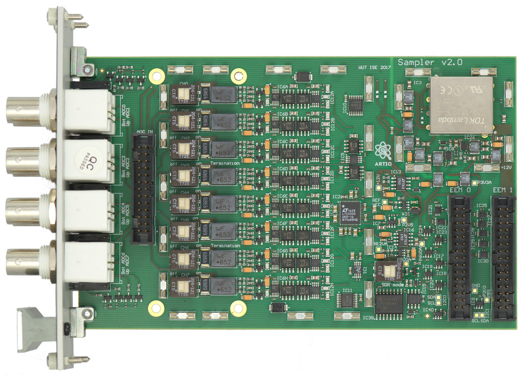
Sampler can be operated either in basic mode as a standard SPI EEM using a single EEM connector (EEM0), or in fast mode via a source-synchronous LVDS interface and 2 EEM connectors (EEM0-EEM1).
In basic mode, the channels must be read out sequentially, in decreasing order. The maximum SPI clock is limited by the round-trip delay in the cabling used to connect Sampler to the master. With a 20 MHz SPI read clock (25ns round trip plus setup), we get one sample one each channel per 6.9us (30ns tCONVH + 450ns tCONV + 8 channels * 16 bits * 50ns).
Fast mode allows all ADC channels to be read out simultaneously at 1.5 MHz via a source-synchronous interface. This is implemented (~ 1 MHz on each channel for all channels) in the Kasli-Sampler-Urukul "SU" laser intensity servo.
EEM connector usage:
| Pin | EEM0 | EEM1 (fast mode only) |
|---|---|---|
| 0 | ADC-SCK | ADC-CLKOUT |
| 1 | ADC-SDOA | ADC-SDOA |
| 2 | ADC-SDR | ADC-SDOB |
| 3 | ADC-CNV | ADC-SDOC |
| 4 | PGIA-SCK | ADC-SDOD |
| 5 | PGIA-MOSI | NC |
| 6 | PGIA-MISO | NC |
| 7 | PGIA-CS | NC |
"PGIA" refers to the front-end programmable-gain instrumentation amplifiers, which are controlled over SPI via a shift register.
Note that on hardware v2.2 the LVDS line driver for PGIA-MISO (IC19) is not populated by default.
To do: check power handling of termination resistors!
Tests performed using Sampler Rev 1.1 prototype hardware. See issue 226 for further details. Further tests will be done on the Rev 2 hardware.
Unless stated otherwise, all measurements use:
- 200kHz ADC clock
- Input termination off for signals connected directly to a voltage source, termination on for "floating" inputs
- PGAI G=1
- Drive an input (termination off) from a signal generator.
- Scan the signal frequency to measure the -6dB frequency on the ADC.
- The sample rate was 125kSPS, so the signal frequency was above the Nyquist frequency for most gain settings.
- Signal was nominally -28dBFS=1Vpp/G (there was a slight error due to the ADC reference gain being incorrect in this hardware revision).
| Gain | Small-signal BW (kHz) |
|---|---|
| 1 | 206 |
| 10 | 207 |
| 100 | 195 |
| 1000 | 87 |
- We made the following measurements, which confirm that the large-signal bandwidth is the same as the small-signal bandwidth to within the measurement accuracy for gains of 1 and 10.
- G=10, 1Vpp=-8.1dBFS: 213kHz
- G=10, 2Vpp=-1.2dBFS: 212kHz
- G=1, 10Vpp=-8.1dBFS: 214kHz
- Sample rate for this measurement was 200kHz, measurement bin width was 3Hz (65k samples)
- We measured the noise spectrum both for a terminated input (0V input) and (using batteries as a low-noise voltage source) for signals close to full-scale. No significant difference observed between the two cases. Data below are all for terminated (0V) inputs.
- No spurs seen above the noise floor at any frequency (e.g. no SMPS spurs seen)
- Noise spectrum is white once DC offset was subtracted
- Measure noise floor as a function of gain
| gain | LSB RMS | µV RMS | nV/rtHz |
|---|---|---|---|
| 1 | 1.3 | 420 | TBD |
| 10 | 1.4 | 44 | TBD |
| 100 | 3.6 | 11 | TBD |
| 1000 | 14.3 | 4.4 | TBD |
DC cross-talk measurement:
- Input A: apply +-17V DC, termination off. NB this voltage is clipped by the protection diodes, but was chosen to really stress-test the design.
- Input B: termination on measure signal level
- With input B G=1, voltage applied to input A makes <1LSB change in level measured at input B. DC cross-talk is thus <96dB.
- To do: re-measure DC cross-talk at G=1k
AC cross-talk measurement:
- Gain was the same on all channels.
- Apply 50kHz, 10Vpp (-8.8dBFS) signal to one channel. NB this saturates the PGIA for G>1!
- Measure signal on the adjacent channel as a function of PGIA gain
- Termination is on for the driven channel, but off for all other channels
- Note that the lack of dependence of the cross-talk on PGIA gain suggests that the cross-talk is dominated by pickup before the PGIA -- most-likely in the BNC connector.
| Gain | Measured signal (dBFS) | Cross-talk (dBc) |
|---|---|---|
| 1 | -87 | -79.2 |
| 10 | -67 | -78.2 |
| 100 | -46 | -77.2 |
| 1000 | -29 | -81.2 |
- With the termination on for all channels, we find:
| Gain | Measured signal (dBFS) | Cross-talk (dBc) |
|---|---|---|
| 1 | <-130 | <-121 |
| 10 | -111.5 | -123 |
| 100 | -93.7 | -124.9 |
| 1000 | -72.2 | -123.4 |
- Short input ground and signal together for one channel
- Apply sinewave to input signal/ground
- Measure the signal level seen by the ADC
| Freq [kHz] | measured signal level [dBFS] | CMRR (dB) |
|---|---|---|
| 0.01 | <-120 | >-98 |
| 0.1 | < -120 | >-98 |
| 1 | <-120 | >-98 |
| 10 | -109 | - 87 |
| 100 | -87 | -55 |
| 1000 | -105 | -83 |
| 10000 | -108 | -85 |
| Freq [kHz] | measured signal level [dBFS] | CMRR (dB) |
|---|---|---|
| 0.01 | <-110 | >-118 |
| 0.1 | -98 | -116 |
| 1 | -88 | - 106 |
| 10 | -70 | - 88 |
| 100 | -50 | - 68 |
| 1000 | -80 | - 98 |
| 10000 | <-100 | >-118 |
- 25kHz signal applied to input
- measure the level of the second harmonic (50kHz) and third harmonic (75kHz) as a function of input signal level.
| Input level | Second harmonic | Third harmonic |
|---|---|---|
| 0.1Vpp (-48dBFs) | -51dBc | |
| 1Vpp (-28dBFs) | -69dBc | |
| 10Vpp (-8dBFs) | -58.8dBc |
If MCX connectors are preferred over BNC then the MCX_BNC_adapter adaptor can be used. This can be installed during manufacture or the conversion can be done by the user. The MCX connectors allow use of a 4HP panel instead of the 8HP required for BNCs.